Vherso by Smart Group Apps SAS Vherso by Smart Group Apps SAS
    #seo #socialmedia #seoservice #usaaccounts #digitalmarketer
    Advanced Search
  • Login
  • Register

  • Night mode
  • © 2026 Vherso by Smart Group Apps SAS
    About • Directory • Contact Us • Developers • Privacy Policy • Terms of Use • Refund

    Select Language

  • Arabic
  • Bengali
  • Chinese
  • Croatian
  • Danish
  • Dutch
  • English
  • Filipino
  • French
  • German
  • Hebrew
  • Hindi
  • Indonesian
  • Italian
  • Japanese
  • Korean
  • Persian
  • Portuguese
  • Russian
  • Spanish
  • Swedish
  • Turkish
  • Urdu
  • Vietnamese

Watch

Watch Reels Movies

Events

Browse Events My events

Blog

Browse articles

Market

Latest Products

Pages

My Pages Liked Pages

More

Forum Explore Popular Posts Games Jobs Offers Fundings
Reels Watch Events Market Blog My Pages See all
University Wafer
User Image
Drag to reposition cover
University Wafer

University Wafer

@universitywafer
  • Timeline
  • Groups
  • Likes
  • Friends 0
  • Photos
  • Videos
  • Reels
  • Products
UniversityWafer, Inc. supplies high-quality silicon and diverse semiconductor substrates—like SOI, GaAs, sapphire, ITO—for research and small-batch production with fast delivery.
0 Friends
10 posts
https://www.universitywafer.com/
Male
Working at University Wafer
Living in United States
Located in 11 Elkins Street Unit 330 , South Boston
image

Claim $5 in SITE – Free Airdrop!

Join the crypto revolution backed by real estate! Get $5 FREE in SITE just for signing up. Real assets. Real rewards. Real simple. ??

Hurry, limited spots available! ⏳

Claim $5 Now
University Wafer
University Wafer
9 w ·Translate

Epitaxial vs. Standard Silicon Wafers: A Complete Guide

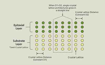
Epitaxy comes from the Greek words "epi" (above) and "taxis" (in an ordered manner), referring to the process of growing a crystalline layer on a crystalline substrate. https://www.universitywafer.co....m/compare-epitaxial-

Compare Epitaxial vs Standard Silicon Wafers | Applications, Structure, Cost
Favicon 
www.universitywafer.com

Compare Epitaxial vs Standard Silicon Wafers | Applications, Structure, Cost

Explore the structural and performance differences between epitaxial and standard silicon wafers. Learn which wafer type is best for power devices, CMOS, and cost-sensitive applications.
Like
Comment
Share
University Wafer
University Wafer
14 w ·Translate

Comparing SOI Wafers vs. Conventional Wafers: A Complete Guide

The main difference between SOI and conventional wafers is how they're built. Regular silicon wafers are made of a single piece of crystal silicon with a polished surface where devices are made. https://www.universitywafer.co....m/soi-wafers-vs-conv

SOI Wafers vs Conventional Silicon | Differences, Performance & Applications
Favicon 
www.universitywafer.com

SOI Wafers vs Conventional Silicon | Differences, Performance & Applications

Compare SOI wafers with conventional silicon wafers. Learn about layer structures, electrical performance, thermal properties, and use in advanced applications.
Like
Comment
Share
University Wafer
University Wafer
17 w ·Translate

Reference Wafers for Calibration Purposes

If you are calibrating metrology tools—such as 4-point probes, eddy current gauges, or contactless resistivity mappers—you rarely need a full cassette of 25 identical wafers.https://www.universitywafer.co....m/reference-wafers.h

Reference Wafers for Metrology & Tool Calibration | UniversityWafer, Inc.
Favicon 
www.universitywafer.com

Reference Wafers for Metrology & Tool Calibration | UniversityWafer, Inc.

Buy single silicon reference wafers for 4-point probe and eddy current calibration. Custom resistivity standards from 0.001 to >10,000 Ohm-cm. No minimum order.
Like
Comment
Share
University Wafer
University Wafer
22 w ·Translate

Optimize Your Wafer Testing Procedures

The semiconductor industry relies heavily on the quality and Silicon Carbide Waferconsistency of silicon wafers and other substrate materials.https://www.universitywafer.co....m/wafer-testing-opti

Wafer Testing Optimization | Improve Semiconductor Yield & Quality
Favicon 
www.universitywafer.com

Wafer Testing Optimization | Improve Semiconductor Yield & Quality

Learn how to optimize wafer testing procedures for silicon, SiC, SOI, and BioMEMS. Reduce defects, improve yield, and ensure semiconductor reliability
Like
Comment
Share
University Wafer
University Wafer
25 w ·Translate

Comprehensive Guide to Wafer Quality Assurance Standards

Quality assurance in wafer manufacturing makes sure semiconductor materials meet the strict requirements needed for research and production.https://www.universitywafer.co....m/quality-assurance-

Wafer Quality Assurance Standards | Silicon, GaAs, Sapphire Inspection
Favicon 
www.universitywafer.com

Wafer Quality Assurance Standards | Silicon, GaAs, Sapphire Inspection

Explore semiconductor wafer quality standards including SEMI, ISO 9001, and inspection techniques for silicon, GaAs, sapphire, and more. Ensure defect-free materials for research and manufacturing.
Like
Comment
Share
Load more posts

Unfriend

Are you sure you want to unfriend?

Report this User

Edit Offer

Add tier


Select an image
Delete your tier
Are you sure you want to delete this tier?

Reviews

In order to sell your content and posts, start by creating a few packages. /home/app_social/vherso1/public_html/themes/wondertag/layout/modals/site-alerts.phtml on line 208

Warning: Trying to access array offset on value of type null in /home/app_social/vherso1/public_html/themes/wondertag/layout/modals/site-alerts.phtml on line 208
https://vherso.com/setting&user=&page=monetization">Monetization

Pay By Wallet

Payment Alert

You are about to purchase the items, do you want to proceed?

Request a Refund